Protecting IoT Gateways from Silent Storage Failure:
Understanding the Limitations of Solid State Storage in Embedded PCs Using Robustel Flash Manager
White Paper – Executive Summary
Brief
Most developers underestimate the hidden risk inside their IoT gateways: NAND Flash wear-out. While eMMC storage offers durability and cost efficiency, it has a finite write/erase cycle — meaning poor software design can silently destroy devices long before their intended service life.
This whitepaper explains why storage failures often strike at scale, outlines how to measure real-world endurance, and introduces Robustel’s Flash Manager — a built-in diagnostic tool for EG5000 series gateways that helps teams detect, test, and mitigate Flash wear before it becomes a field failure.
The takeaway: with proactive monitoring and empathetic software design, organizations can extend device lifetimes, reduce warranty costs, and ensure reliable IoT operations.
What you’ll learn
- The endurance limitations of MLC NAND Flash, and why unmanaged writes accelerate failure .
- Key differences between eMMC and SD cards, and why industrial gateways should rely on eMMC .
- How Linux I/O stacks, write amplification, and workload patterns directly impact Flash health.
- Practical strategies — over-provisioning, write optimization, pSLC options — to extend storage lifetime.
- How to use Robustel Flash Manager to monitor wear, run stress tests, and forecast device longevity.

Introduction
NAND Flash has become a de facto storage medium for modern day consumer devices such as cellphones, tablet PCs and e-readers. It is also the bulk storage medium inside SSDs, USB drives and SD cards and a common inclusion in low-cost embedded computers like Robustel’s EG5000 series.
Devices made using NAND Flash offer mechanical shock resistance, high durability and are able to withstand high temperature and pressure, making them ideal for industrial applications. A common form-factor for NAND Flash storage within industrial systems like Robustel’s EG5000 series Edge Gateways is “eMMC”.
NAND flash is a popular nonvolatile memory, mainly because of its small size, low power consumption and durability. Although this technology is suitable for pure ‘storage’, many important features need to be considered when it is included in a complex system especially one that is running an Operating System like Linux.
Compared to traditional hard disk drives, eMMC has no moving parts so it’s ideal for systems that vibrate and shake. NAND Flash also offers fast read access times, which is crucial for data intensive applications. However, one of the main drawbacks of NAND Flash based storage is the relatively limited number of write/erase cycles that such a device can withstand.
Put simply, a NAND Flash device ‘wears out’, and its rate of wear is proportional to how much it is used – it is conceptually similar to a battery, except there is no practical way to recharge an eMMC drive.
Many System Integrators/developers are not aware of the “Endurance” limitations of MLC NAND Flash, and this can cause premature failure of entire fleets of IoT devices. So, it is critical to measure how your software behaves and mitigate the issues associated with unsympathetic application software design when MLC NAND Flash is used or the primary storage device – especially one hosting a Linux OS & application software.
This white-paper is designed to help developers understand how to measure the impact of their software on an eMMC (NAND Flash) drive & what can be done if it appears that premature ‘wear-out’ is a risk for your application.
A brief note on eMMC vs SD Cards
A number of very low-cost embedded PCs will use an SD Card as the primary storage medium, containing all critical OS and application files.
Some of the challenges of SD vs eMMC that are worth considering include:
An eMMC chip soldered to the PCB will have much better vibration resistance than an SD card stuck into a slot/holder
An eMMC chip will have a better cybersecurity implication as it cannot be easily removed from the product
The tight clearance between the eMMC chip and the PCB reduces unwanted inductance and signal distortion, which tends to allow higher data-transfer rates than SD cards.
Another concern with SD cards is the large number of fakes on the market, which sometimes find their way into even legitimate products. Something in an eMMC package is much more traceable and less likely to be part of a fake product venture.
Robustel’s products only use eMMC chips for the primary OS, but some products can accommodate an SD card for low cost bulk storage.
Chapter 1: Understanding “Wear” at the physical layer
Flash memory is made of a unique arrangement of logic gates set up in a feedback loop, and these logic gates are made of transistors. The transistors are fabricated all together on one piece of silicon foundation, with layers of etching and additives to the silicon to create the design pattern and the electrical properties needed to form the components. This one-piece device is known as an integrated circuit. This IC fabrication process is similar to other applications such as other types of memory, CPUs, controllers, and graphics processors.
Flash memory wears out, unlike other IC components which never really wear out unless there is an event that causes damage to part of it, such as overheating or an electrical surge. Flash wear is due to the unique requirement by design, that the “erasing process hits the flash cell with a relatively large charge of electrical energy.” Flash drives can’t simply overwrite bytes of data, as with magnetic discs. Instead, it has to clear out whole blocks at a time, analogous to sectors on a magnetic disc, in order to write new data. Each time a block is erased, the large electrical charge actually degrades the silicon material a minute amount, until after enough write-erase cyles, the electrical properties of the flash cell begin to break down and that cell becomes unreliable.
So, by design, NAND Flash has many great properties including cost and durability but the trade-off is a finite lifetime per block, hence application developers must preserve the available resource through empathetic use of the chip.
Chapter 2: Measuring “Wear” from the host system
This is where things start to get a little more complicated.
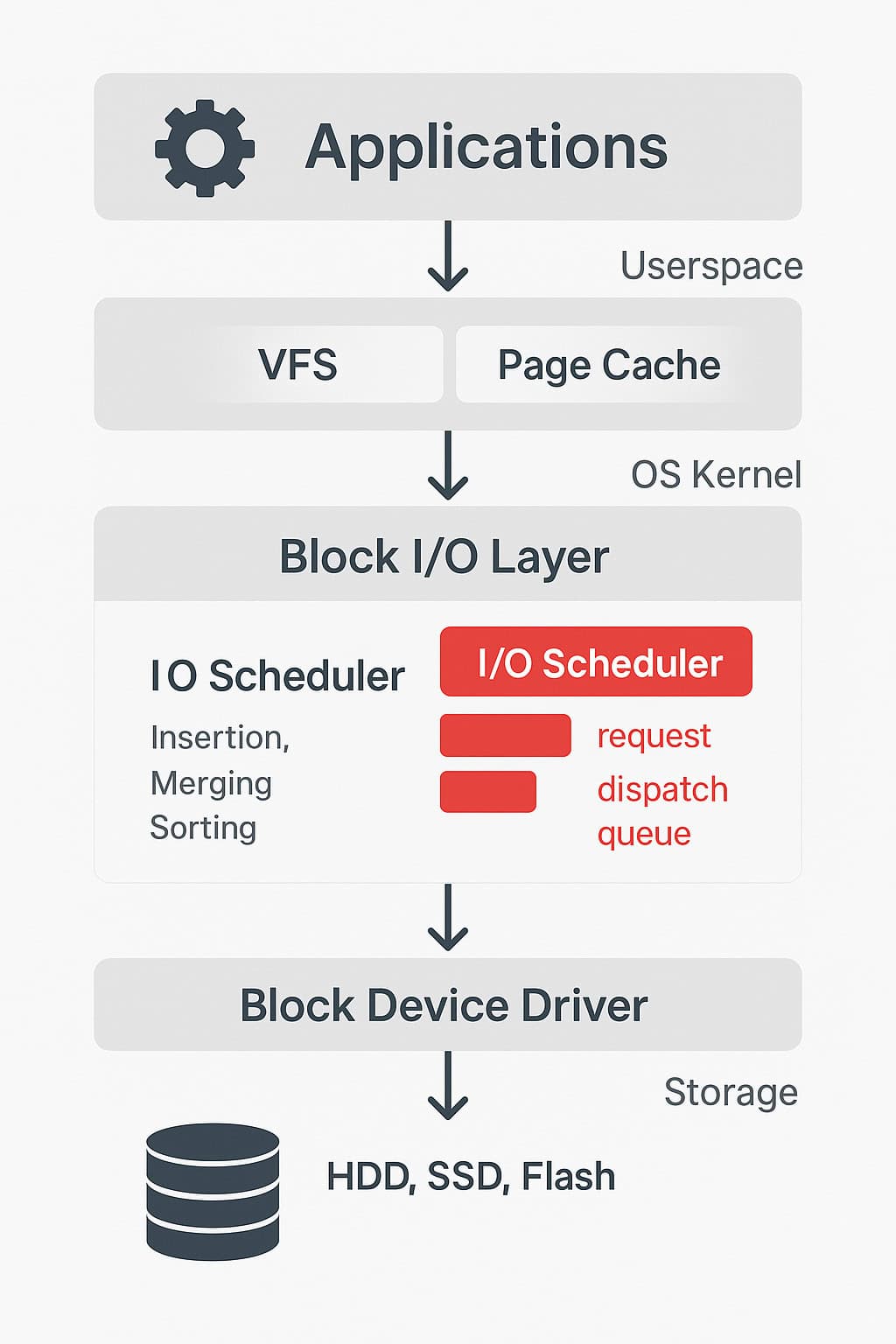
The Linux I/O stack comprises a complex array of subsystems working in tandem to optimize read/write performance from User-space to hardware and back. It is not always clear which user-level writes hit the Flash memory or how.
The NAND Flash device – eMMC or SSD will have its own controller inside that is configured to prolong device lifetime by optimising when and how writes are made to Flash.
There are several tools inside a Linux OS that can help to shine light on what is happening and where. Please note before reading on in this chapter, trying to establish exactly how your code flows through the IO stack might not be the most expedient solution to a complex problem so some readers can consider
the rest of this Chapter as being for information only. Subsequent chapters highlight more practical real-world solutions for managing risk without becoming a Linux IO expert!
Here are some examples of functions in Linux that could help with your analysis:
iostat
The iostat command is used for monitoring system input/output device loading by observing the time the devices are active in relation to their average transfer rates. The iostat command generates reports that can be used to change system configuration to better understand the input/output load of physical disks – eg. eMMC Flash.
iotop
iotop is a common Linux command. It is a ‘top’-like utility for disk input and output (I/O). Use this command to see I/O usage information output by the Linux kernel. It displays a table of current I/O usage by Linux processes or threads on the Linux system.
blktrace & blkparse
blktrace is particularly useful as it gives layer-wise information from inside the block I/O layer. When used correctly, it’s possible to generate events for all I/O requests and monitor it from where it is evolving. Though it extracts data from the kernel, it is not an analysis tool and the interpretation of the data can be complex. Developers can feed the output from blktrace into tools like btt or blkparse to get the analysis done.
Chapter 3: Measuring “Wear” at Drive level
An eMMC storage device comprises of NAND Flash chips and a “Device Controller”. The controller is the heart of the device and is there to optimise the I/O reads and writes so performance and endurance are optimal when used with modern operating systems.
Key functions of the Controller include Block Management, Garbage Collection, Error Control and Wear Levelling. The reader might find it useful to further research these topics to fully understand NAND Flash management.
1)Jedec standard health reporting introduced in JEDEC v5.0 gives an estimated remaining lifetime in 10% increments but is not very granular. It is a useful in-service tool for a coarse approximation of device wear but is not a very good pre-deployment diagnostic tool to fully understand and assess risk associated with premature wear out of Flash.
2)eMMC devices contain Vendor specific registers that indicate useful real-time data such as number of block erases & increased bad clock count.
Because these can change on a per-vendor basis, working out exactly how to interrogate Device Controllers can take a little time. The explicit commands are sometimes not included in the User Guide and/or only available under NDA.
The mmc-utils tool in Linux is part of this story – it is commonly used to interrogate eMMC devices from Linux to achieve the following:
- Set the eMMC write protect status.
- Create a general-purpose partition.
- Permanently enable/disable the eMMC H/W Reset feature.
- Print and parse CSD (Card Specific Data) information.
- Print and parse extCSD (Extended Card Specific Data) infomation.
The last two items of the list above are the most relevant to this paper as they give a general idea of how to print/read information from an eMMC chip, especially that pertaining to device health.
Readers that are interested in the most granular detail on this subject should now interrogate the manufacturer or the manufacturer’s documentation for their chosen NAND Flash based device to understand what health related data is included and how to access it. “CMD56” is a commonly used generic command for this information.
Because of the vagaries and complexities of the above, Robustel have developed the “Flash Manager” application that runs on all EG5000 series Gateways to allow customers to easily retrieve useful eMMC-related health information. More on this in Chapter 6.
Because of the vagaries and complexities of the above, Robustel have developed the “Flash Manager” application that runs on all EG5000 series Gateways to allow customers to easily retrieve useful eMMC-related health information. More on this in Chapter 6.
Chapter 4: The equation for NAND Flash wear/endurance
A good coarse approximation of estimated device life is TBW = Total Bytes Written. The governing equation is as follows:
TBW = DC * EF / WAF
Where:
DC = Device Capacity in Bytes
EF = Endurance Factor = maximum program/erase cycles (as defined by Flash type – 3000 for typical MLC NAND Flash as used in Robustel products)
WAF = Write Amplification Factor (application / setup specific)
A simple analysis of above shows that DC and EF should be large and WAF should be small for the best possible TBW or “endurance” of the Flash devices. We will now explain these concepts in detail and how to achieve maximum endurance.
- DC = Device Capacity
This is a simple concept. eMMC are shipped in typical sizes of 1GB, 2GB, 4GB etc.
Choosing a device that has lots of extra capacity compared with what the OS/application requires is a simple way to create higher endurance. This is known as “over-provisioning”.
- EF = Endurance Factor
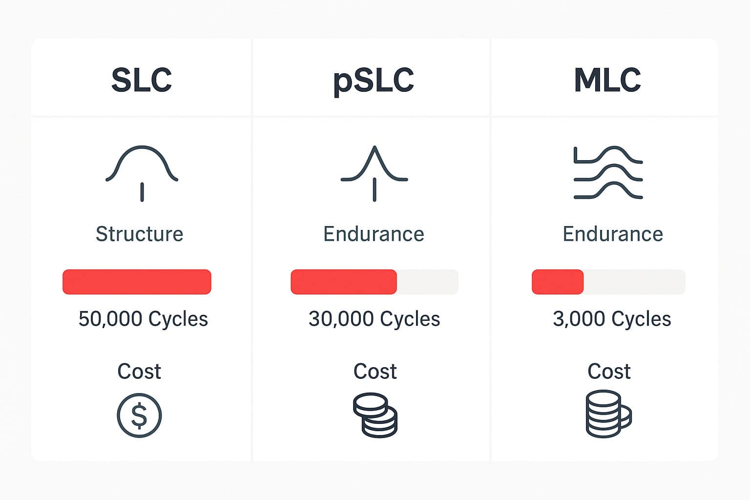
Figure 1.1 shows typical values for this in the row marked P/E cycles. The majority of mainstream eMMC devices use “MLC” NAND Flash with an EF of 3000.
It is possible to change to an “SLC” NAND Flash device to bring about a substantial and direct increase in endurance thanks to SLC’s 100,000 P/E cycles but it is not commonly used in low cost/high volume IoT Devices due to cost.
With the highest “cost per bit” of all Flash types, SLC is typically only used in high criticality applications like Military, Aerospace and Enterprise IT.
The choice here for the product designer is simple – use expensive SLC to increase endurance or be smart about the application of MLC NAND Flash. Most consumer/industrial applications apply the latter principle.
- WAF = Write Amplification Factor
This entire white-paper and its objectives pivot on this critical concept.
Understanding and subsequently reducing the WAF of your application software is the cheapest way to improve endurance, but it is not a trivial concept.
Write amplification (WA) is an undesirable phenomenon associated with flash memory and solid-state drives (SSDs) where the actual amount of information physically written to the storage media is a multiple of the logical amount intended to be written.
Because flash memory must be erased before it can be rewritten, with much coarser granularity of the erase operation when compared to the write operation, the process to perform these operations results in moving (or rewriting) user data and metadata more than once. Thus, rewriting some data requires an already-used-portion of flash to be read, updated, and written to a new location, together with initially erasing the new location if it was previously used. Due to the way flash works, much larger portions of flash must be erased and rewritten than actually required by the amount of new data. This multiplying effect increases the number of writes required over the life of the SSD, which shortens the time it can operate reliably. The increased writes also consume bandwidth to the flash memory, which reduces write performance to the SSD. Many factors will affect the WA of an SSD; some can be controlled by the user and some are a direct result of the data written to and usage of the SSD.
Above is the start of an excellent article on this subject on Wikipedia – see: http://en.wikipedia.org/wiki/Write_amplification
We recommend the reader takes time to read this article, particular the section entitled “Factors affecting the value” as this is where there are some detailed concepts that can be explored by Developers to decrease WAF and hence increase eMMC endurance.
One of the simplest ways application developers can try to optimise their software is to encourage disk writes to be large and sequential as opposed to short and random. This will help to keep the WAF in the typical 4 to 8 range as opposed to some applications whose WAF can be significantly higher.
It can be helpful to develop your system assuming a very bad WAF of 20. If your calculations show that your NAND Flash device will have sufficient endurance for the lifetime of the project, then you can be quite confident that the outcome will be positive.
Chapter 5: General methods for Reducing & Managing “Wear”
A – Over-provisioning
One of the simplest methods to prevent NAND Flash wearing out is to have more of it. Robustel’s EG5100 Gateway has 8GB, and the EG5120 has 16GB eMMC NAND Flash. This is a relatively large amount of storage for such devices, driving up baseline product cost, but it’s one of the most simple and effective ways of increasing lifetime.
If we use a typical WAF of 6 for the EG5100 and EG5120 respectively, we get Endurance (TBW) figures of:
EG5100 – (8589934592 x 3000/6) = 3.9TBW
EG5120 – (17179869184 x 3000/6) = 7.8 TBW
If we assume product life is 5 years,
that’s 5 x 365 = 1825 days
This means that the EG5120 could handle 7.8/1825*1024 = 4.4GB worth of writes per day for 5 years.
However, with poorly implemented software with a WAF of 18, that figure would drop to one third of that with only 1.5GB per day able to be written, which corresponds to only 64MB per hour – a relatively small number for a modern OS.
B – Understand Write Amplification
Encourage your application developers to study this excellent article: https://en.wikipedia.org/wiki/Write_amplification
We could not hope to better this narrative on the subject so please make the most of it!
C – Use pSLC to increase endurance
Like most of the embedded PC industry, Robustel uses MLC NAND Flash to keep costs competitive but Robustel can also offer “pSLC” for applications where there is concern about the endurance of the system Storage (NAND Flash) for long life-time applications.
This is available from Robustel on a “per project” basis – your Robustel rep can provide more information.
D – Other Considerations
i) A simple way to improve Flash lifetime may be to limit “debug” and “logging” information as this is often written on the fly
ii) Designing your application to use write-once patterns for data that does not change frequently. If data is only appended and never modified, it reduces wear.
iii) Allowing the data in the NAND flash to fill close to capacity – therefore requiring more program/erase cycles needed to move data around before sufficient pages are marked for erasure is not recommended.
iv) Remember that the specific strategies you choose may depend on the nature of your application and the type of data it manages.
Chapter 6: Introducing Flash Manager – Robustel’s wear monitoring utility
All of Robustel’s EG5000 series (and other RobustOS PRO) series gateways include a “Flash Manager” feature that allows developers to quickly ascertain NAND Flash status without needing detailed knowledge of Linux commands that interrogate Flash device Controllers.
Flash Manager allows customers to deploy an image onto an EG5000 series and measure NAND Flash performance before and after a period of operation in ‘typical’ conditions.
By comparing NAND Flash state before and after and then extrapolating out that rate of wear to an expected product lifetime, it’s possible for product developers to quickly ascertain that their software writes to eMMC in an empathetic way and products will not suffer from premature failure for NAND Flash wear reasons.
Robustel interrogate both the JEDEC standard health status and vendor proprietary registers to provide as detailed a snapshot as possible.
By comparing successive snapshots against time elapsed, application developers can get a feeling for real-world endurance and assure themselves that the hardware and software can last for the required lifetime of the project.
Detailed Overview of Flash Manager
By comparing successive snapshots against time elapsed, application developers can get a feeling for real-world endurance and assure themselves that the hardware and software can last for the required lifetime of the project.
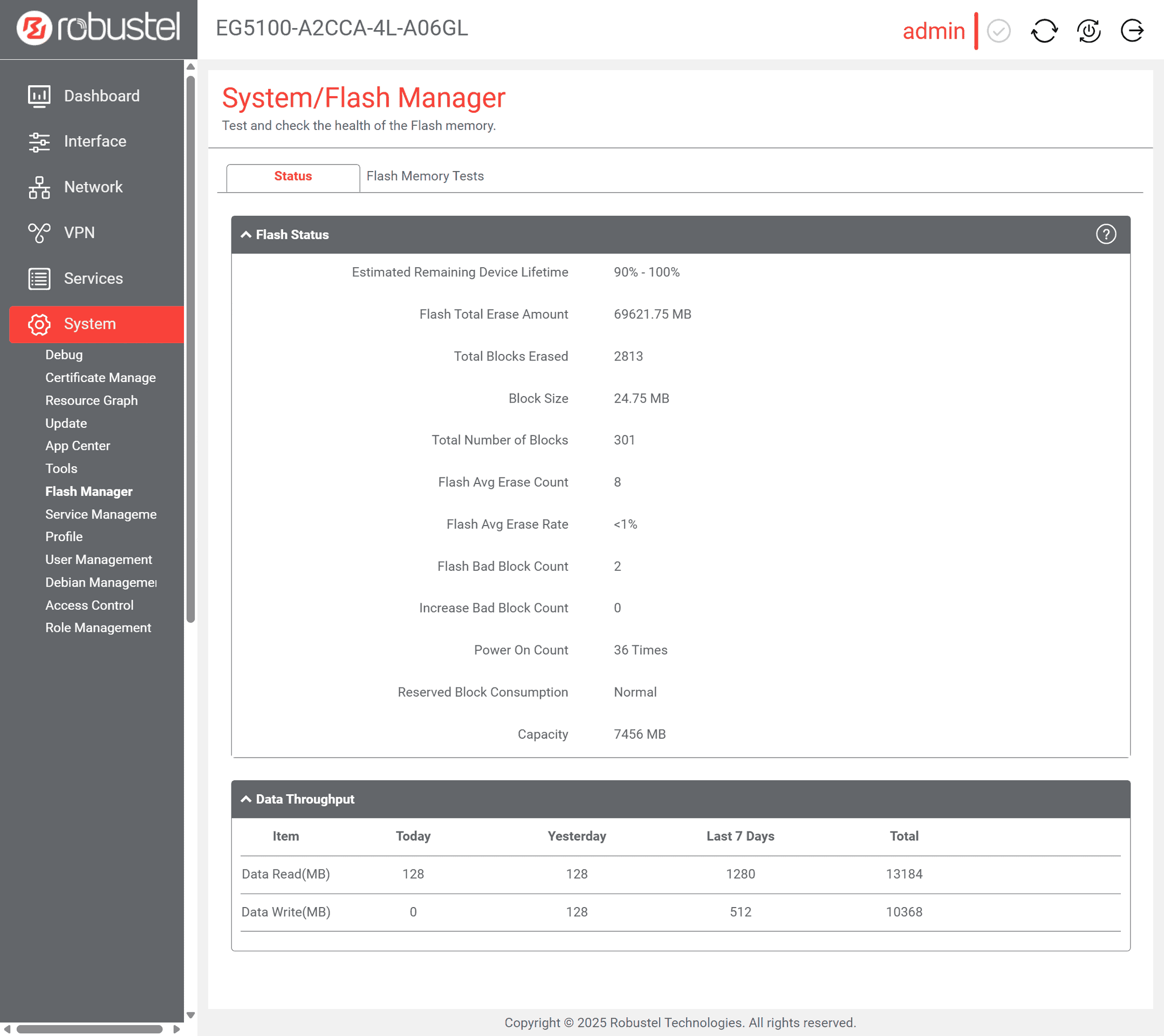
A – Status screen
Per screenshot below, the status screen keeps a running total of useful NAND flash parameters. These are explained in more detail shortly.
B – Flash Memory Tests
A Flash Memory Test can be set running by the user for a period of up to 14 days duration.
It can be manually started or scheduled to start at a specific time.
The output of a test is a CSV file with a detailed comparison of NAND Flash status at the beginning and at the end of the test. This result can be analysed and extrapolated to the useful lifetime of the system deployment.
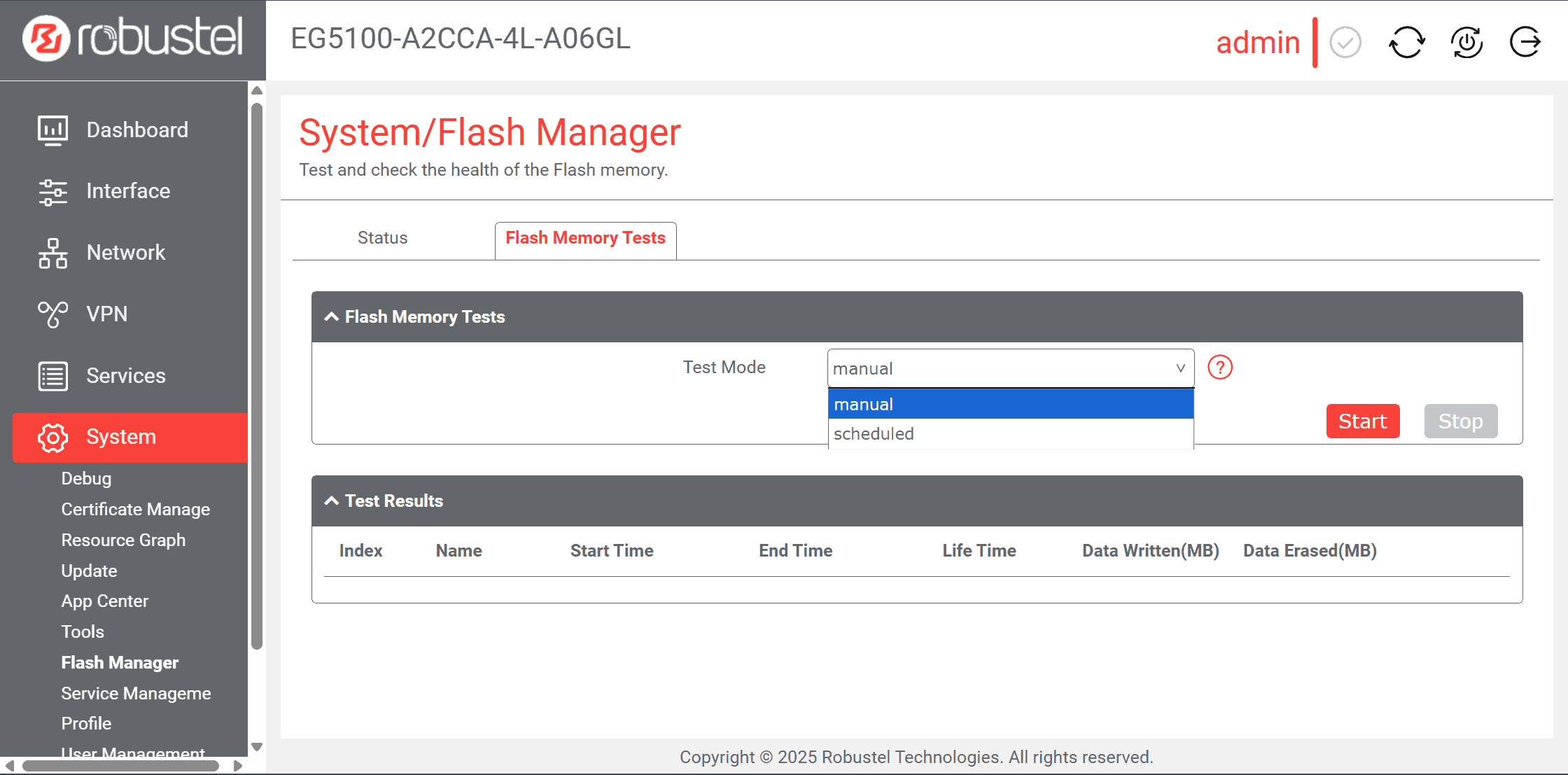
C – Test result analysis
The output from a test is per the CSV file below. Underneath, we explain the meaning and significance of each line.
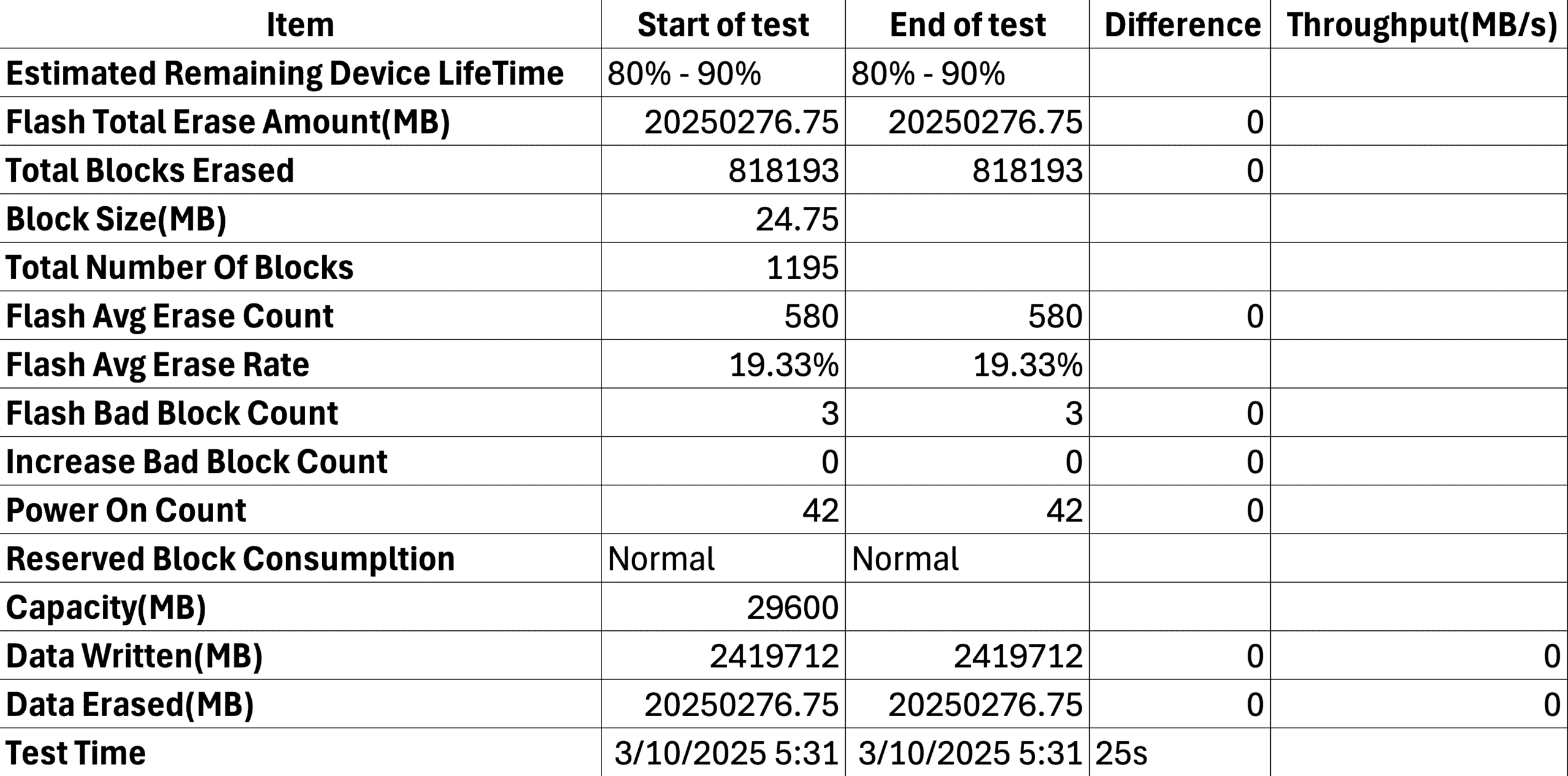
- Estimated Remaining Device LifeTime = This is a coarse approximation of expected remaining lifetime of a NAND Flash device. It is based on the JEDEC standard JESD84-A43.
- Flash Total Erase Amount(MB) = Total amount of data erased during the test based on Total Blocks erased multiplied by Block Size.
- Total Blocks Erased = The total number of Block erase actions during the test. This is arguably the most important variable by far when getting a feel for how well your device will survive based on the currently running software.
- Block Size(MB) = Block size of NAND Flash device (usually eMMC) per the current configuration. A block comprises of a number of “pages”.
- Total Number Of Blocks = Total number of Blocks that the NAND Flash is made up of.
- Flash Avg Erase Count = Number of Block Erase actions per usable block as an average The maximum avg erase count is 3000 for MLC NAND flash.
- Flash Avg Erase Rate = Average number of erase counts divided by total number of blocks.
- Flash Bad Block Count = Total number of “bad blocks” as detected by the Flash controller.
- Increase Bad Block Count = How many blocks became “bad” during the test.
- Power On Count = How many times has the NAND Flash/eMMC device been powered up.
- Reserved Block Consumption = When a bad block is generated, a reserved block is used to replace the bad block to ensure the reliability of the NAND flash. After all reserved blocks are used to replace bad blocks, if bad blocks are generated, no reserved block can be used to replace the bad block.
- Capacity(MB) = Total device capacity – does not change. For reference only.
- Data Written(MB) = Total data written to the device (as measured by the controller) during the test.
- Data Erased(MB) = Total data erased from the device (as measured by the controller) during the test.
D – Applying Flash Manager results
Using the start and end figures from the report, we can easily estimate how the user’s application will affect the health of the flash memory in the EG5000 series over an extended period by extrapolating out the results given over the duration of the test.
Appendix A – Warranty conditions for EG5000 series products
“Robustel Gateways are warrantied against premature failure within the first 2 years of their life as standard but failure due to excessive wear/use of NAND Flash is NOT covered by the standard warranty. eMMC module replacemement may be possible in some conditions but this will always be a chargeable service available at Robustel’s sole discretion.”
Partner with Robustel: Your Expert Ally in Industrial IoT
Managing Flash endurance is not just about extending hardware life — it’s about building IoT systems that your business can trust long-term. At Robustel, we combine deep industry expertise with proven tools like Flash Manager to help you anticipate risks, reduce costs, and keep operations running smoothly. Partner with us today and gain a trusted ally in navigating the complexities of industrial IoT.